SLVSAW1A June 2011 – January 2017 TPS65053-Q1
PRODUCTION DATA.
- 1 Features
- 2 Applications
- 3 Description
- 4 Revision History
- 5 Pin Configuration and Function
- 6 Specifications
- 7 Detailed Description
- 8 Application and Implementation
- 9 Power Supply Recommendations
- 10Layout
- 11Device and Documentation Support
- 12Mechanical, Packaging, and Orderable Information
パッケージ・オプション
メカニカル・データ(パッケージ|ピン)
- RGE|24
サーマルパッド・メカニカル・データ
- RGE|24
発注情報
1 Features
- Qualified for Automotive Applications
- AEC-Q100 Qualified With the Following Results:
- Device Temperature Grade 3: –40°C to +85°C Ambient Operating Temperature Range
- Device HBM ESD Classification Level 2
- Device CDM ESD Classification Level C4B
- Up To 95% Efficiency
- Output Current for DC-DC Converters:
- DCDC1 = 1 A; DCDC2 = 0.6 A
- DC-DC Converters Externally Adjustable
- VIN Range for DC-DC Converters
From 2.5 V to 6 V - 2.25-MHz Fixed Frequency Operation
- Power Save Mode at Light-Load Current
- 180° Out-of-Phase Operation
- Output Voltage Accuracy in PWM Mode ±1%
- Total Typical 32-μA Quiescent Current for Both DC-DC Converters
- 100% Duty Cycle for Lowest Dropout
- One General-Purpose 400-mA LDO
- Two General-Purpose 200-mA LDOs
- VIN Range for LDOs from 1.5 V to 6.5 V
- Output Voltage for LDO3:
- VLDO3 = 1.3 V
- Available in a 4-mm × 4-mm 24-Pin VQFN Package
2 Applications
- Automotive Li-Ion Battery-Powered Devices
- GPS, Emergency Cell Phone
- Digital Cameras
- Satellite Radio Modules
- OMAP™ and Low-Power DSP
3 Description
The TPS65053-Q1 device is integrated power management IC (PMIC) for applications powered by one Li-Ion or Li-Polymer cell, which require multiple power rails. The TPS65053-Q1 device provides two highly efficient, 2.25-MHz step-down converters targeted at providing the core voltage and I/O voltage in a processor-based system. Both step-down converters enter a low power mode at light loads for maximum efficiency across the widest possible range of load currents. For low-noise applications, the devices can be forced into fixed-frequency PWM mode by pulling the MODE pin high. Both converters allow the use of small inductors and capacitors to achieve a small solution size.
The TPS65053-Q1 device provides an output current of up to 1 A on the DCDC1 converter and up to 0.6 A on the DCDC2 converter. The device also integrates one 400-mA LDO and two 200-mA LDO voltage regulators, which can be turned on and off using separate enable pins on each LDO. Each LDO operates with an input voltage range from 1.5 V to 6.5 V, allowing them to be supplied from one of the step-down converters or directly from the main battery. LDO1 and LDO2 are externally adjustable, while LDO3 has a fixed output voltage of 1.3 V.
The TPS65053-Q1 device is available in a small 24-pin leadless package (4-mm × 4-mm VQFN) with a 0,5-mm pitch.
Device Information(1)
| PART NUMBER | PACKAGE | BODY SIZE (NOM) |
|---|---|---|
| TPS65053-Q1 | VQFN (24) | 4.00 mm × 4.00 mm |
- For all available packages, see the orderable addendum at the end of the data sheet.
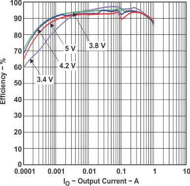
Efficiency of DCDC1

4 Revision History
Changes from * Revision (June 2011) to A Revision
- Added the Device Information table, ESD Ratings table, Feature Description section, Device Functional Modes, Application and Implementation section, Power Supply Recommendations section, Layout section, Device and Documentation Support section, and Mechanical, Packaging, and Orderable Information sectionGo
- Deleted all references to TPS650531-Q1 and TPS650532-Q1 devices Go
- Changed values in the Thermal Information table to align with JEDEC standards.Go