SLVSAL1E March 2011 – April 2016 TPS24720
PRODUCTION DATA.
- 1 Features
- 2 Applications
- 3 Description
- 4 Revision History
- 5 Pin Configuration and Functions
- 6 Specifications
-
7 Detailed Description
- 7.1 Overview
- 7.2 Functional Block Diagram
- 7.3 Feature Description
- 7.4
Device Functional Modes
- 7.4.1 Board Plug-In
- 7.4.2 Inrush Operation
- 7.4.3 Action of the Constant-Power Engine
- 7.4.4 Circuit Breaker and Fast Trip
- 7.4.5 Automatic Restart
- 7.4.6 PGb, FLTb, and Timer Operations
- 7.4.7 Overtemperature Shutdown
- 7.4.8 Start-Up of Hot-Swap Circuit by VCC or EN
- 7.4.9 Minimization of Power Dissipation at STANDY by ENSD
- 7.4.10 Fault Detection of MOSFET Short With FFLTb
-
8 Application and Implementation
- 8.1 Application Information
- 8.2
Typical Application
- 8.2.1 Design Requirements
- 8.2.2
Detailed Design Procedure
- 8.2.2.1
Power-Limited Start-Up
- 8.2.2.1.1 STEP 1. Choose RSENSE, RSET, and RIMON
- 8.2.2.1.2 STEP 2. Choose MOSFET M1
- 8.2.2.1.3 STEP 3. Choose Power-Limit Value, PLIM, and RPROG
- 8.2.2.1.4 STEP 4. Choose Output Voltage Rising Time, tON, and Timing Capacitor CT
- 8.2.2.1.5 STEP 5. Calculate the Retry-Mode Duty Ratio
- 8.2.2.1.6 STEP 6. Select R1, R2, and R3 for UV and OV
- 8.2.2.1.7 STEP 7. Choose RGATE, R4, R5, R6, and C1
- 8.2.2.2 Additional Design Considerations
- 8.2.2.1
Power-Limited Start-Up
- 8.2.3 Application Curve
- 9 Power Supply Recommendations
- 10Layout
- 11Device and Documentation Support
- 12Mechanical, Packaging, and Orderable Information
パッケージ・オプション
メカニカル・データ(パッケージ|ピン)
- RGT|16
サーマルパッド・メカニカル・データ
- RGT|16
発注情報
1 Features
- 2.5-V to 18-V Operation
- Accurate Current Limiting for Startup
- Programmable FET SOA Protection
- Adjustable Current Sense Threshold
- Programmable Fault Timer
- Power-Good Output
- Fast Breaker for Short-Circuit Protection
- Analog Load-Current Monitor Output
- Programmable UV and OV
- Low-current Standby Mode
- FET Fault Detection Flag
- 3-mm × 3-mm, 16-Pin QFN package
2 Applications
- Server Backplanes
- Storage Area Networks (SAN)
- Telecommunications Mezzanine Cards
- Medical Systems
- Plug-In Modules
- Base Stations
3 Description
The TPS24720 is an easy-to-use, full-featured protection device for 2.5-V to 18-V power rails. This hot-swap controller drives an external N-channel MOSFET, while protecting source, load and external MOSFET against multiple potentially damaging events. During startup, load current and MOSFET power dissipation are limited to user-selected values. After startup, currents above the user-selected limit will be allowed to flow until programmed timeout – except in extreme overload events when load is immediately disconnected from source.
Programmable power limiting ensures the external MOSFET operates inside its safe operating area (SOA) at all times. This allows use of smaller FETs while improving system reliability. Power good, Fault, FET Fault, and current monitor outputs are provided for system status monitoring and downstream load control.
Device Information(1)
| PART NUMBER | PACKAGE | BODY SIZE (NOM) |
|---|---|---|
| TPS24720 | VQFN (16) | 3.00 mm × 3.00 mm |
- For all available packages, see the orderable addendum at the end of the data sheet.
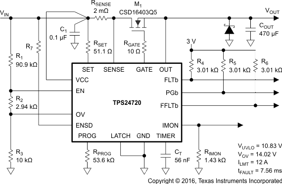
Typical Application (12 V at 10 A)
